Top Products Wafer Prober PCP-102WS

Double Sided Wafer Prober
PCP-102WS


Outline

The PCP-102WS is a high precision prober designed to contact both sides (double side) of wafer.
By adopting PFC original XY Compensation and Profiling function, PCP-102WS can compensate the position even if a wafer is warped.
Accurate RDS (on-resistance) is measured by making Kelvin connection at the drain side on the back of wafer and adjusting its drain-sense-position to the source-sense-position.


FEATURES

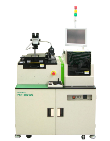
Contacts both sides (double side) of wafer
Effective position compensation for the warpage of wafer
Successful record 100% of Alignment for customers' products (Record only in Japan)
Measures the accurate RDS (on-resistance)
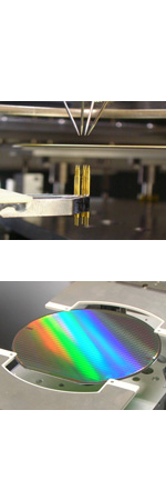
Probing at more than two points by moving in a chip (Micro Probing)
Large current/High voltage probing is supported by the wafer clamp system with ceramic blade
Low noise: More than -80dB on the chuck
(Reference Value: 30KHZ to 30MHZ Loop ANT actual measurement)
High rigidity cabinet made by the iron surface plate and the welding frame realizes low vibration
Low cost and High throughput
Small space (Footprint), power-saving design
Stable operation (more than MTBF5000 hours)


OPTIONS

Large diameter Pre-alignment chuck can handle a warped wafer, thin wafer and TAIKO™ Wafer


SPECIFICATION

Wafer size 100mm (4 inch) to 200mm (8 inch)
Probing area Wafer: φ200mm
XY stage Driven by linear motor (Repeat accuracy:1um)
Footprint Small space: (W)1200mm × (D)860mm


OTHERS

Sales achievement: PCP series more than 500 sets (As of April 2022)
We can respond to the request from a customer flexibly.
We can offer discount for the purchase of several sets together.

 Products
for more information
Site Map | Terms of Use | Privacy Policy © Plum Five Co., Ltd.